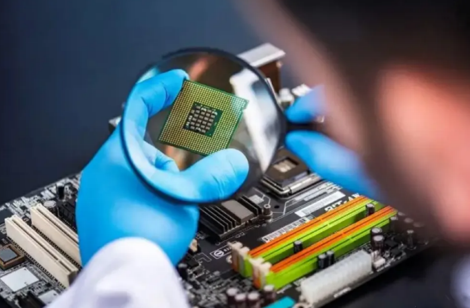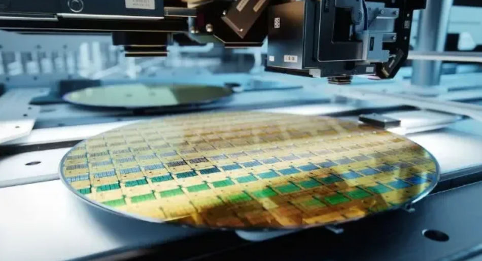
Packaging and testing involves dicing, wire bonding, and plastic encapsulating qualified wafers. This ensures electrical connections between the chip circuits and external devices, provides mechanical and physical protection for the chip, and utilizes testing tools to test the functionality and performance of the packaged chip.
The packaging and testing phase is of great significance
Obtaining an IC chip requires a lengthy process, from design to manufacturing. However, chips are extremely small and thin, and without external protection, they can be easily scratched and damaged.

Packaging and testing (P&T) positions, secures, seals, and protects chips, enhancing electrical and thermal performance. It also serves as a bridge between the chip's internal world and external circuitry. Wires connect the chip's contacts to pins on the packaging and testing enclosure, and these pins, in turn, connect to other components via wires on the printed circuit board. Therefore, P&T plays a crucial role in integrated circuits.
Main Process of P&T
Wafer acceptance testing (WAT) is an electrical test performed by the wafer foundry before shipment. Wafers that pass the WAT are sent to the P&T facility.
The P&T facility first performs chip probe (CP) testing on the wafers. Due to various manufacturing defects introduced during the manufacturing process, a certain amount of defective products may be present in the bare die on the wafer. The CP test is designed to identify these defects before packaging, reducing subsequent P&T costs.

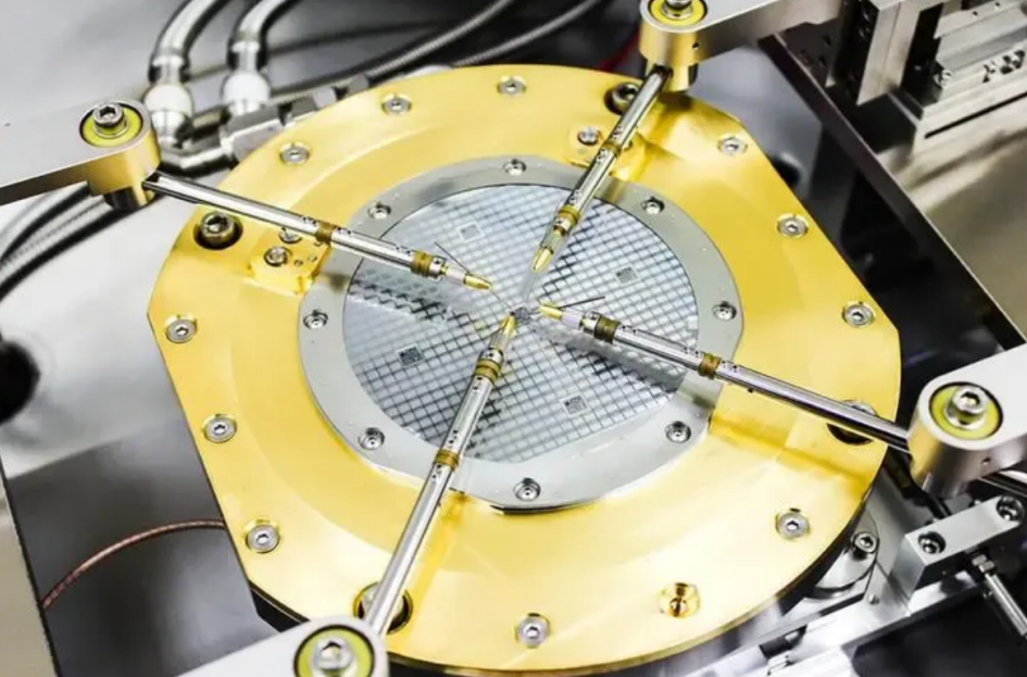
After wafer fabrication, probes contact the chip pads to test chip functionality, flagging any defective chips and screening them after dicing.
Air-floating platforms are used for wafer dicing
The probe station, consisting of a stage, optical components, and a chuck, primarily handles transport and positioning, allowing wafers to sequentially contact the probes for testing. It provides automated wafer loading and unloading, centering, alignment, and positioning, and moves the wafer according to a designed step size to ensure the probes on the probe card align with the corresponding locations on the silicon wafer for testing.

The stage is a component used to position wafers or chips. It's typically designed to fit the wafer's dimensions and equipped with precise motion and positioning capabilities. Our independently developed ultra-precision air flotation platform serves as the stage, boasting a repeatability of ±50nm. This provides ultra-precise mechanical motion and positioning for precise wafer positioning and inspection.
After completing the CP test, the packaging process begins. The packaging process is generally divided into two parts: the steps before plastic encapsulation are called the front-end operation, and the steps after molding are called the back-end operation.
The main process flow for packaging and testing is as follows:
1. Front-end
Wafer grinding: The backside of the freshly processed wafer is thinned to the required thickness for packaging. During backside grinding, tape is applied to the front side to protect the circuit area. After grinding, the tape is removed.
Wafer sawing: The wafer is mounted on a blue film and then cut into individual dices, which are then cleaned.
Optical Inspection: Checks for defective products.
Die Attach: Die attachment, silver paste curing (to prevent oxidation), and wire bonding.
II. Back-end Process
Injection Molding: Protects against external impact, seals and tests the product with EMC (molding compound), and heat-hardens it.
Laser Marking: Inscribes information on the product, such as the production date and batch number.
High-Temperature Curing: Protects the IC's internal structure and eliminates internal stress.
Flash Removal: Trims edges and corners.
Electroplating: Improves conductivity and enhances solderability.
Slicing and Molding: Checks for defective products.
This completes the chip packaging and testing process. The process flow varies depending on the packaging technology, and testing is also performed during the packaging process. After packaging, the product undergoes Final Test (FT). Only products that pass FT testing can be shipped.
Share