PCB component placement is not a matter of personal whim; there are specific rules that must be followed. In addition to general requirements, certain specialized components have their own distinct placement guidelines.
Layout requirements for press-fit components
1) For right-angle male/female press-fit components, no components taller than 3 mm may be placed within a 3 mm radius, and no soldered components may be placed within a 1.5 mm radius; on the opposite side of the board, no components may be placed within 2.5 mm of the center of the press-fit pin holes.
2) For straight male/female press-fit components, no components may be placed within a 1 mm radius. If a shroud is to be installed on the back of the component, no components may be placed within 1 mm of the shroud's edge; if no shroud is used, no components may be placed within 2.5 mm of the press-fit holes.
3) For live-pluggable grounding connectors used with Euro-style connectors, a keep-out zone extends 6.5 mm from the tip of long pins and 2.0 mm from the tip of short pins.
4) For 2mmFB power single-pin connectors, a keep-out zone extends 8 mm from the tip of the long pin (relative to the mating board-side socket).
Layout requirements for heat-sensitive components
1) During component layout, keep heat-sensitive components (such as electrolytic capacitors, crystal oscillators, etc.) as far away as possible from high-heat components.
2) Heat-sensitive components should be placed close to the element being monitored but away from high-temperature zones to avoid interference from other heat-generating components that could cause malfunctions.
3) Place components that generate heat but are heat-resistant near air outlets or at the top of the assembly; however, if a component cannot withstand high temperatures, place it near the air inlet. Ensure that heat-generating components and heat-sensitive components are offset from one another along the path of rising airflow.
Layout requirements for polarized components
1) Polarized or directional through-hole devices (THD) should be oriented consistently and arranged neatly.
2) Polarized surface-mount components (SMC) should have consistent orientation on the board; components of the same type should be arranged neatly and aesthetically.
(Polarized components include: electrolytic capacitors, tantalum capacitors, diodes, etc.)
Layout requirements for through-hole reflow (THR) components
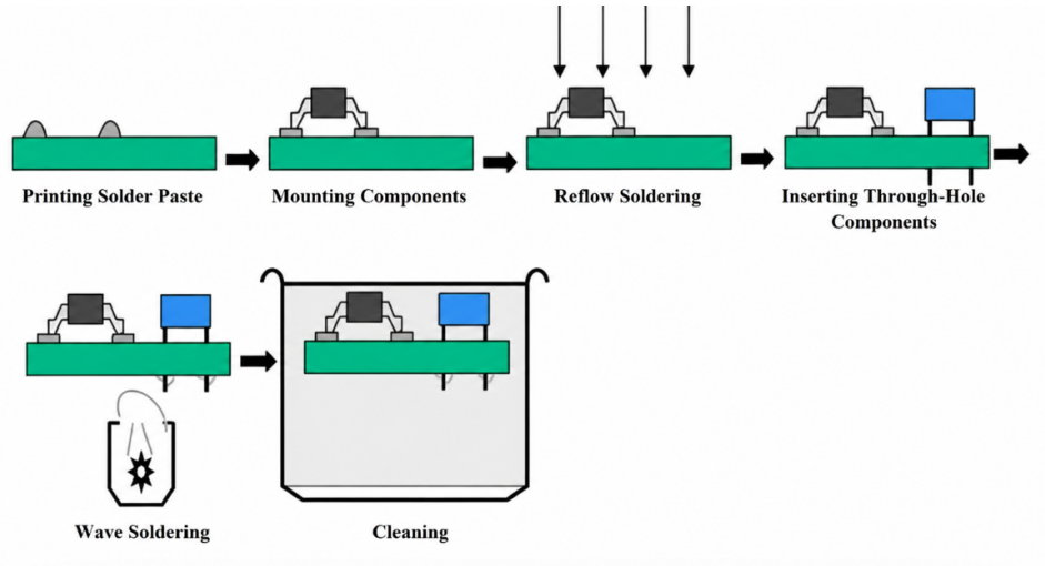
1) For PCBs with non-conveyor edges exceeding 300 mm in length, avoid placing heavy components in the center of the board whenever possible. This minimizes PCB deformation caused by the weight of through-hole components during soldering and reduces the impact of the insertion process on components already mounted on the board.
2) To facilitate the insertion process, it is recommended to place components near the side where insertion operations are performed.
3) For long components (such as memory sockets), it is recommended to align their long axis with the direction of board transport.
4) Maintain a distance of more than 20 mm between the pad edges of through-hole reflow components and QFPs, SOPs, connectors, or BGAs with a pitch of ≤0.65 mm. The distance to other SMT components should be greater than 2 mm.
5) Maintain a distance of more than 10 mm between the bodies of through-hole reflow components.
6) The distance from the pad edges of through-hole reflow components to the conveyor edge must be ≥10 mm, and the distance to non-conveyor edges must be ≥5 mm.
Share