Wire bonding is the most important internal connection method in MEMS device packaging, currently accounting for over 90% of all connections. It uses extremely fine metal wires (typically 18-50μm in diameter) to create atomic-scale bonds between the metal wires and the MEMS chip pads and substrate pads, utilizing heat, pressure, ultrasonic energy, or a combination thereof. This allows for electrical interconnection and signal transmission between the chip and external circuits. Wire bonding for MEMS chips primarily utilizes the same bonding techniques used for IC chips. The basic process involves first sintering the wire ends into small balls, which are then pressure-bonded to the chip's solder joints (the first solder joint). The wires are then pulled along a designed path and finally pressure-bonded to the corresponding solder joints on the substrate (the second solder joint). Simultaneously, the wires are broken and new balls are formed, preparing the way for the next wire. Bonding types primarily include thermocompression bonding, ultrasonic bonding.

Figure 1 Schematic diagram of the lead process
Common bonding wire materials include gold (Au), aluminum (Al), copper (Cu) and silver (Ag) alloy wires. Au wires have stable chemical properties, are not easily oxidized, have good conductivity and plasticity, and have the most mature technology. However, Au is expensive and easily forms intermetallic compounds with aluminum pads, affecting long-term reliability. Al wires are cheap, but are easily oxidized, have low mechanical strength and high resistivity, poor thermal conductivity, and larger solder joints. Cu wires are extremely easy to oxidize, and bonding requires greater ultrasonic energy and pressure. They are generally used more in mid- and low-end products.

Figure 2 Schematic diagram of MEMS chip wire bonding
In MEMS, common lead diameters range from 18μm to 50μm (approximately 0.7mil to 2mil). The most common pad material is aluminum, though Au pads are also used in high-reliability applications. The pad side length should be at least 1.5 times the lead ball diameter. Based on empirical data, for leads with diameters between 25µm and 50µm, the minimum pad size is typically designed between 60µm × 60µm and 100µm × 100µm. For fine-pitch applications, the edge spacing between adjacent pads is typically required to be at least 25µm.
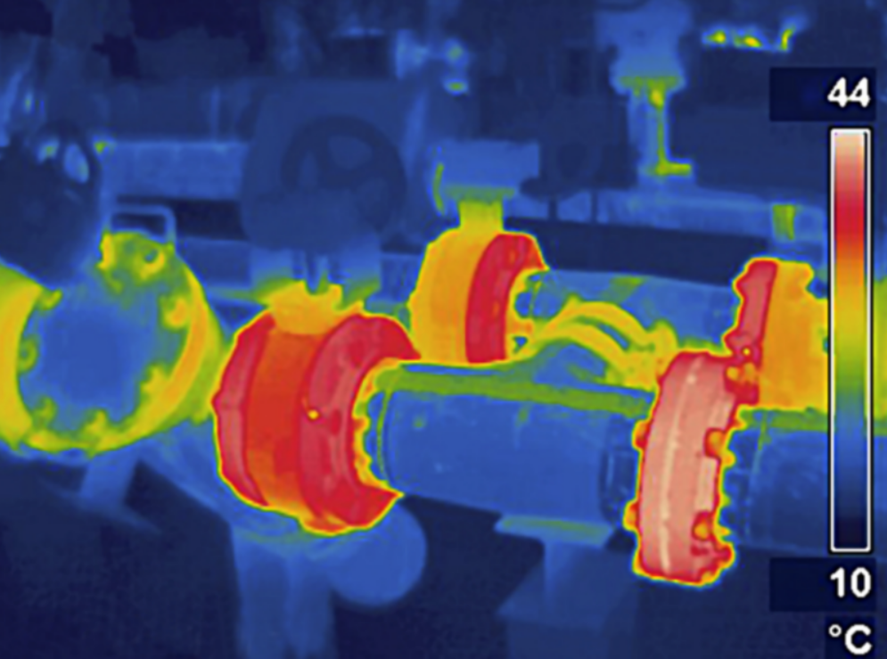
The core of a pressure sensor is the pressure-sensing diaphragm. Heat and mechanical stress during the bonding process can be transferred to the diaphragm, causing sensor zero drift or sensitivity changes. Therefore, low-temperature bonding processes such as thermosonic bonding should be preferred, and the lead curvature should be optimized to reduce stress on the chip. RF MEMS switches are used to process high-frequency signals. The leads themselves have parasitic inductance and capacitance, which can affect signal quality. To minimize these parasitic effects, the leads must be as short as possible, and the loop height must be as low and consistent as possible. The placement and loop height of the bond wires for optical devices such as MEMS micromirrors must not block the light path or interfere with the optical signal. Accelerometers and gyroscopes contain movable masses and precision suspension structures, making them extremely sensitive to external mechanical shock and vibration. Ultrasonic vibrations during bonding can damage these structures.

Figure 3 Gold wire bonding of optical device micromirror
Share